-
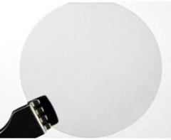
Polished wafer
FZ polished wafers, mainly for the production of silicon rectifier (SR), silicon controlled rectifier (SCR), Giant Transistor (GTR), thyristor (GRO)Hot Tags : Polished wafer Polished Silicon Wafer Wafer MEMS Technology Wafer Electronics Silicon Material
-
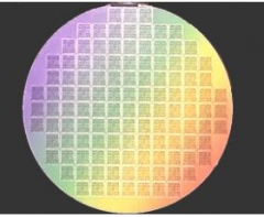
Etching wafer
The etching wafer has the characteristics of low roughness, good glossiness and relatively low cost, and directly substitutes the polished wafer or epitaxial wafer which has relatively high cost to produce the electronic elements in some fields, to reduce the costs. There are the low-roughness, low-reflectivity and high-reflectivity etching wafers.Hot Tags : Etching Wafer Etching Silicon Wafer MEMS Plasma Etching Etching Process PECVD
-
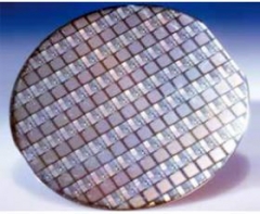
Photo Mask
PAM-XIAMEN Offers Photomasks A photo mask is a thin coating of masking material supported by a thicker substrate, and the masking material absorbs light to varying degrees and can be patterned with a custom design. The pattern is used to modulate light and transfer the pattern through the process of photolithography which is the fundamental process used to build almost all of today’s digital devices.Hot Tags : Photo Mask Photomask Photomask Manufacturing Photomask Printing Photolithography Mask Printing


 Contact Information
 +86-592-5601 404