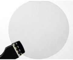
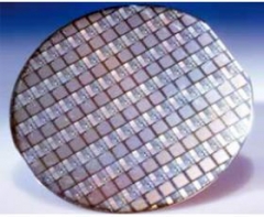
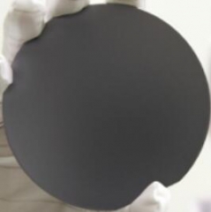
Xiamen Powerway offers GaSb wafer - gallium antimonide which are grown by LEC(Liquid Encapsulated Czochralski) as epi-ready or mechanical grade with n type, p type or semi-insulating in different orientation(111)or(100)
MOQ :
1Xiamen Powerway offers GaSb wafer - gallium antimonide which are grown by LEC(Liquid Encapsulated Czochralski) as epi-ready or mechanical grade with n type, p type or semi-insulating in different orientation(111)or(100).
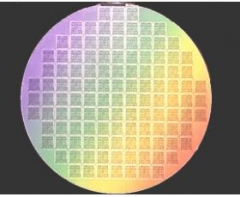
Gallium antimonide (GaSb) is a semiconducting compound of gallium and antimony of the III-V family.It has a lattice constant of about 0.61 nm. GaSb can be used for Infrared detectors,infrared LEDs and lasers and transistors, and thermophotovoltaic systems.
Wafer Specification
Item
Specifications
Wafer Diameter
2"50.5±0.5mm
3"76.2±0.4mm
4"1000.0±0.5mm
Crystal Orientation
(100)±0.1°
Thickness
2"500±25um
3" 625±25um
4"1000±25um
Primary flat length
2"16±2mm
3"22±2mm
4"32.5±2.5mm
Secondary flat length
2"8±1mm
3"11±1mm
4"18±1mm
Surface Finish
P/E, P/P
Package
Epi-Ready,Single wafer container or CF cassette
| Electrical and Doping Specification | |||||
| Conduction Type | p-type | p-type | n-type | n-type | n-type |
| Dopant | Undoped | Zinc | Tellurium | Low tellurium | High tellurium |
| E.D.P cm-2 |
2"≤2000 3"≤5000 |
2"≤2000 3"≤5000 |
2",3"≤1000 4"≤2000 |
2"≤1000 3",4"≤2000 |
2,"3",4"≤500 |
| Mobility cm² V-1s-1 | ≥500 | 450-200 | 3500-2000 | 3500-2000 | 3500-2000 |
| Carrier Concentration cm-3 | ≤2*1017 | ≥1*1018 | (91-900)*1017 | ≤2*1017 |
≥5*1017 |
Remark:
The Chinese government has announced new limits on the exportation of Gallium materials (such as GaAs, GaN, Ga2O3, GaP, InGaAs, and GaSb) and Germanium materials used to make semiconductor chips. Starting from August 1, 2023, exporting these materials is only allowed if we obtains a license from the Chinese Ministry of Commerce. Hope for your understanding and cooperation!
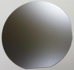
Xiamen Powerway offers InSb wafer - Indium antimonide which are grown by LEC(Liquid Encapsulated Czochralski) as epi-ready or mechanical grade with n type, p type or semi-insulating in different orientation(111)or(100).
Xiamen Powerway offers InP wafer - Indium Phosphide which are grown by LEC(Liquid Encapsulated Czochralski) or VGF(Vertical Gradient Freeze) as epi-ready or mechanical grade with n type, p type or semi-insulating in different orientation(111)or(100).
Xiamen Powerway offers InAs wafer - Indium arsenide which are grown by LEC(Liquid Encapsulated Czochralski) as epi-ready or mechanical grade with n type, p type or semi-insulating in different orientation(111)or(100).
Xiamen Powerway offers GaP wafer - gallium Phosphide which are grown by LEC(Liquid Encapsulated Czochralski) as epi-ready or mechanical grade with n type, p type or semi-insulating in different orientation(111)or(100).
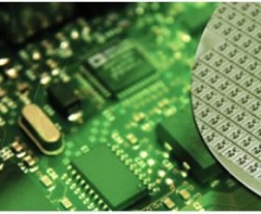
Due to SiC physical and electronic properties,Silicon Carbide based device are well suitable for short wavelength optoelectronic, high temperature, radiation resistant, and high-power/high-frequency electronic devices,compared with Si and GaAs based device.
Xiamen Powerway offers InAs wafer - Indium arsenide which are grown by LEC(Liquid Encapsulated Czochralski) as epi-ready or mechanical grade with n type, p type or semi-insulating in different orientation(111)or(100).
PAM-XIAMEN offers semiconductor silicon carbide wafers,6H SiC and 4H SiC in different quality grades for researcher and industry manufacturers. We has developed SiC crystal growth technology and SiC crystal wafer processing technology,established a production line to manufacturer SiC substrate,Which is applied in GaN epitaxy device,power devices,hi1
FZ polished wafers, mainly for the production of silicon rectifier (SR), silicon controlled rectifier (SCR), Giant Transistor (GTR), thyristor (GRO)
 Contact Information
 luna@powerwaywafer.compowerwaymaterial@gmail.com
  +86-592-5601 404