PAM-XIAMEN offers semiconductor silicon carbide wafers,6H SiC and 4H SiC in different quality grades for researcher and industry manufacturers. We has developed SiC crystal growth technology and SiC crystal wafer processing technology,established a production line to manufacturer SiC substrate,Which is applied in GaN epitaxy device,power devices,high-temperature device and optoelectronic Devices. As a professional company invested by the leading manufacturers from the fields of advanced and high-tech material research and state institutes and China's Semiconductor Lab,we are devoted to continuously improve the quality of currently substrates and develop large size substrates.
MOQ :
1
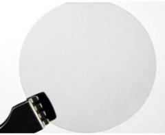
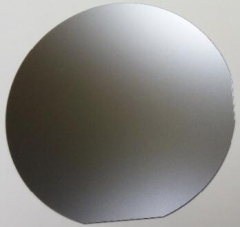
Silicon Carbide Wafers
PAM-XIAMEN offers semiconductor silicon carbide wafers,6H SiC and 4H SiC in different quality grades for researcher and industry manufacturers. We has developed SiC crystal growth technology and SiC crystal wafer processing technology,established a production line to manufacturer SiC substrate,Which is applied in GaN epitaxy device,power devices,high-temperature device and optoelectronic Devices. As a professional company invested by the leading manufacturers from the fields of advanced and high-tech material research and state institutes and China's Semiconductor Lab,we are devoted to continuously improve the quality of currently substrates and develop large size substrates.
Here shows detail specification:
SILICON CARBIDE MATERIAL PROPERTIES
|
Polytype |
Single Crystal 4H |
Single Crystal 6H |
|
Lattice Parameters |
a=3.076 Å |
a=3.073 Å |
|
|
c=10.053 Å |
c=15.117 Å |
|
Stacking Sequence |
ABCB |
ABCACB |
|
Band-gap |
3.26 eV |
3.03 eV |
|
Density |
3.21 · 103 kg/m3 |
3.21 · 103 kg/m3 |
|
Therm. Expansion Coefficient |
4-5×10⁻⁶/K |
4-5×10⁻⁶/K |
|
Refraction Index |
no = 2.719 |
no = 2.707 |
|
|
ne = 2.777 |
ne = 2.755 |
|
Dielectric Constant |
9.6 |
9.66 |
|
Thermal Conductivity |
490 W/mK |
490 W/mK |
|
Break-Down Electrical Field |
2-4 · 108 V/m |
2-4 · 108 V/m |
|
Saturation Drift Velocity |
2.0 · 105 m/s |
2.0 · 105 m/s |
|
Electron Mobility |
800 cm2/V·S |
400 cm2/V·S |
|
hole Mobility |
115 cm2/V·S |
90 cm2/V·S |
|
Mohs Hardness |
~9 |
~9 |
6H N-TYPE SIC, 2″WAFER SPECIFICATION
|
SUBSTRATE PROPERTY |
S6H-51-N-PWAM-250 S6H-51-N-PWAM-330 S6H-51-N-PWAM-430 |
|
Description |
A/B Production Grade C/D Research Grade D Dummy Grade 6H SiC Substrate |
|
Polytype |
6H |
|
Diameter |
(50.8 ± 0.38) mm |
|
Thickness |
(250 ± 25) μm (330 ± 25) μm (430 ± 25) μm |
|
Carrier Type |
n-type |
|
Dopant |
Nitrogen |
|
Resistivity (RT) |
0.02 ~ 0.1 Ω·cm |
|
Surface Roughness |
< 0.5 nm (Si-face CMP Epi-ready); <1 nm (C- face Optical polish) |
|
FWHM |
A<30 arcsec B/C/D <50 arcsec |
|
Micropipe Density |
A+≤1cm-2 A≤10cm-2 B≤30cm-2 C≤50cm-2 D≤100cm-2 |
|
Surface Orientation |
|
|
On axis |
<0001>± 0.5° |
|
Off axis |
3.5° toward <11-20>± 0.5° |
|
Primary flat orientation |
Parallel {1-100} ± 5° |
|
Primary flat length |
16.00 ± 1.70 mm |
|
Secondary flat orientation |
Si-face:90° cw. from orientation flat ± 5° |
|
C-face:90° ccw. from orientation flat ± 5° |
|
|
Secondary flat length |
8.00 ± 1.70 mm |
|
Surface Finish |
Single or double face polished |
|
Packaging |
Single wafer box or multi wafer box |
|
Usable area |
≥ 90 % |
|
Edge exclusion |
1 mm |
4H SEMI-INSULATING SIC, 2″WAFER SPECIFICATION
(High-Purity Semi-Insulating(HPSI) SiC substrate is available)
|
SUBSTRATE PROPERTY |
S4H-51-SI-PWAM-250 S4H-51-SI-PWAM-330 S4H-51-SI-PWAM-430 |
|
Description |
A/B Production Grade C/D Research Grade D Dummy Grade 4H SEMI Substrate |
|
Polytype |
4H |
|
Diameter |
(50.8 ± 0.38) mm |
|
Thickness |
(250 ± 25) μm (330 ± 25) μm (430 ± 25) μm |
|
Resistivity (RT) |
>1E5 Ω·cm |
|
Surface Roughness |
< 0.5 nm (Si-face CMP Epi-ready); <1 nm (C- face Optical polish) |
|
FWHM |
A<30 arcsec B/C/D <50 arcsec |
|
Micropipe Density |
A+≤1cm-2 A≤10cm-2 B≤30cm-2 C≤50cm-2 D≤100cm-2 |
|
Surface Orientation |
|
|
On axis <0001>± 0.5° |
|
|
Off axis 3.5° toward <11-20>± 0.5° |
|
|
Primary flat orientation |
Parallel {1-100} ± 5° |
|
Primary flat length |
16.00 ± 1.70 mm |
|
Secondary flat orientation Si-face:90° cw. from orientation flat ± 5° |
|
|
C-face:90° ccw. from orientation flat ± 5° |
|
|
Secondary flat length |
8.00 ± 1.70 mm |
|
Surface Finish |
Single or double face polished |
|
Packaging |
Single wafer box or multi wafer box |
|
Usable area |
≥ 90 % |
|
Edge exclusion |
1 mm |
4H N-type or Semi-insulating SIC,5mm*5mm, 10mm*10mm WAFER SPECIFICATION : Thickness:330μm/430μm
4H N-type or Semi-insulating SIC,15mm*15mm, 20mm*20mm WAFER SPECIFICATION: Thickness:330μm/430μm
4H N-TYPE SIC, 2″WAFER SPECIFICATION
|
SUBSTRATE PROPERTY |
S4H-51-N-PWAM-330 S4H-51-N-PWAM-430 |
|
|
Description |
A/B Production Grade C/D Research Grade D Dummy Grade 4H SiC Substrate |
|
|
Polytype |
4H |
|
|
Diameter |
(50.8 ± 0.38) mm |
|
|
Thickness |
(250 ± 25) μm (330 ± 25) μm (430 ± 25) μm |
|
|
Carrier Type |
n-type |
|
|
Dopant |
Nitrogen |
|
|
Resistivity (RT) |
0.012 - 0.0028 Ω·cm |
|
|
Surface Roughness |
< 0.5 nm (Si-face CMP Epi-ready); <1 nm (C- face Optical polish) |
|
|
FWHM |
A<30 arcsec B/C/D <50 arcsec |
|
|
Micropipe Density |
A+≤1cm-2 A≤10cm-2 B≤30cm-2 C≤50cm-2 D≤100cm-2 |
|
|
Surface Orientation |
|
|
|
On axis |
<0001>± 0.5° |
|
|
Off axis |
4°or 8° toward <11-20>± 0.5° |
|
|
Primary flat orientation |
Parallel {1-100} ± 5° |
|
|
Primary flat length |
16.00 ± 1.70) mm |
|
|
Secondary flat orientation |
Si-face:90° cw. from orientation flat ± 5° |
|
|
C-face:90° ccw. from orientation flat ± 5° |
||
|
Secondary flat length |
8.00 ± 1.70 mm |
|
|
Surface Finish |
Single or double face polished |
|
|
Packaging |
Single wafer box or multi wafer box |
|
|
Usable area |
≥ 90 % |
|
|
Edge exclusion |
1 mm |
|
4H N-TYPE SIC, 3″WAFER SPECIFICATION
|
SUBSTRATE PROPERTY |
S4H-76-N-PWAM-330 S4H-76-N-PWAM-430 |
|
Description |
A/B Production Grade C/D Research Grade D Dummy Grade 4H SiC Substrate |
|
Polytype |
4H |
|
Diameter |
(76.2 ± 0.38) mm |
|
Thickness |
(350 ± 25) μm (430 ± 25) μm |
|
Carrier Type |
n-type |
|
Dopant |
Nitrogen |
|
Resistivity (RT) |
0.015 - 0.028Ω·cm |
|
Surface Roughness |
< 0.5 nm (Si-face CMP Epi-ready); <1 nm (C- face Optical polish) |
|
FWHM |
A<30 arcsec B/C/D <50 arcsec |
|
Micropipe Density |
A+≤1cm-2 A≤10cm-2 B≤30cm-2 C≤50cm-2 D≤100cm-2 |
|
TTV/Bow /Warp |
<25μm |
|
Surface Orientation |
|
|
On axis |
<0001>± 0.5° |
|
Off axis |
4°or 8° toward <11-20>± 0.5° |
|
Primary flat orientation |
<11-20>±5.0° |
|
Primary flat length |
22.22 mm±3.17mm |
|
0.875″±0.125″ |
|
|
Secondary flat orientation |
Si-face:90° cw. from orientation flat ± 5° |
|
C-face:90° ccw. from orientation flat ± 5° |
|
|
Secondary flat length |
11.00 ± 1.70 mm |
|
Surface Finish |
Single or double face polished |
|
Packaging |
Single wafer box or multi wafer box |
|
Scratch |
None |
|
Usable area |
≥ 90 % |
|
Edge exclusion |
2mm |
4H SEMI-INSULATING SIC, 3″WAFER SPECIFICATION
(High Purity Semi-Insulating(HPSI) SiC substrate is available)
|
SUBSTRATE PROPERTY |
S4H-76-N-PWAM-330 S4H-76-N-PWAM-430 |
|
Description |
A/B Production Grade C/D Research Grade D Dummy Grade 4H SiC Substrate |
|
Polytype |
4H |
|
Diameter |
(76.2 ± 0.38) mm |
|
Thickness |
(350 ± 25) μm (430 ± 25) μm |
|
Carrier Type |
semi-insulating |
|
Dopant |
V |
|
Resistivity (RT) |
>1E5 Ω·cm |
|
Surface Roughness |
< 0.5 nm (Si-face CMP Epi-ready); <1 nm (C- face Optical polish) |
|
FWHM |
A<30 arcsec B/C/D <50 arcsec |
|
Micropipe Density |
A+≤1cm-2 A≤10cm-2 B≤30cm-2 C≤50cm-2 D≤100cm-2 |
|
TTV/Bow /Warp |
<25μm |
|
Surface Orientation |
|
|
On axis |
<0001>± 0.5° |
|
Off axis |
4°or 8° toward <11-20>± 0.5° |
|
Primary flat orientation |
<11-20>±5.0° |
|
Primary flat length |
22.22 mm±3.17mm |
|
0.875″±0.125″ |
|
|
Secondary flat orientation |
Si-face:90° cw. from orientation flat ± 5° |
|
C-face:90° ccw. from orientation flat ± 5° |
|
|
Secondary flat length |
11.00 ± 1.70 mm |
|
Surface Finish |
Single or double face polished |
|
Packaging |
Single wafer box or multi wafer box |
|
Scratch |
None |
|
Usable area |
≥ 90 % |
|
Edge exclusion |
2mm |
4H N-TYPE SIC, 4″WAFER SPECIFICATION
|
SUBSTRATE PROPERTY |
S4H-100-N-PWAM-330 S4H-100-N-PWAM-430 |
|
Description |
A/B Production Grade C/D Research Grade D Dummy Grade 4H SiC Substrate |
|
Polytype |
4H |
|
Diameter |
(100.8 ± 0.38) mm |
|
Thickness |
(350 ± 25) μm (430 ± 25) μm |
|
Carrier Type |
n-type |
|
Dopant |
Nitrogen |
|
Resistivity (RT) |
0.015 - 0.028Ω·cm |
|
Surface Roughness |
< 0.5 nm (Si-face CMP Epi-ready); <1 nm (C- face Optical polish) |
|
FWHM |
A<30 arcsec B/C/D <50 arcsec |
|
Micropipe Density |
A+≤1cm-2 A≤10cm-2 B≤30cm-2 C≤50cm-2 D≤100cm-2 |
|
TTV/Bow /Warp |
<45μm |
|
Surface Orientation |
|
|
On axis |
<0001>± 0.5° |
|
Off axis |
4°or 8° toward <11-20>± 0.5° |
|
Primary flat orientation |
<11-20>±5.0° |
|
Primary flat length |
32.50 mm±2.00mm |
|
Secondary flat orientation |
Si-face:90° cw. from orientation flat ± 5° |
|
C-face:90° ccw. from orientation flat ± 5° |
|
|
Secondary flat length |
18.00 ± 2.00 mm |
|
Surface Finish |
Single or double face polished |
|
Packaging |
Single wafer box or multi wafer box |
|
Scratch |
None |
|
Usable area |
≥ 90 % |
|
Edge exclusion |
2mm |
4H N-type or semi-insulating SIC,5mm*5mm, 10mm*10mm WAFER SPECIFICATION: Thickness:330μm/430μm
4H N-type or semi-insulating SIC,15mm*15mm, 20mm*20mm WAFER SPECIFICATION:Thickness:330μm/430μm
a-plane SiC Wafer, size: 40mm*10mm,30mm*10mm,20mm*10mm,10mm*10mm,specs below:
6H/4H N type Thickness:330μm/430μm or custom
6H/4H Semi-insulating Thickness:330μm/430μm or custom
4H SIC,SEMI-INSULATING, 4″WAFER SPECIFICATION
(High-Purity Semi-Insulating(HPSI) SiC substrate is available)
|
SUBSTRATE PROPERTY |
S4H-100-SI-PWAM-350 S4H-100-SI-PWAM-500 |
|
|
Description |
A/B Production Grade C/D Research Grade D Dummy Grade 4H SiC Substrate |
|
|
Polytype |
4H |
|
|
Diameter |
(100 ± 0.5) mm |
|
|
Thickness |
(350 ± 25) μm (500 ± 25) μm |
|
|
Carrier Type |
Semi-insulating |
|
|
Dopant |
V |
|
|
Resistivity (RT) |
>1E5 Ω·cm |
|
|
Surface Roughness |
< 0.5 nm (Si-face CMP Epi-ready); <1 nm (C- face Optical polish) |
|
|
FWHM |
A<30 arcsec B/C/D <50 arcsec |
|
|
Micropipe Density |
A≤5cm-2 B≤15cm-2 C≤50cm-2 D≤100cm-2 |
|
|
TTV/Bow /Warp |
TTV<10μm;TTV< 25μm;WARP<45μm |
|
|
Surface Orientation |
||
|
On axis |
<0001>± 0.5° |
|
|
Off axis |
None |
|
|
Primary flat orientation |
<11-20>±5.0° |
|
|
Primary flat length |
32.50 mm±2.00mm |
|
|
Secondary flat orientation |
Si-face:90° cw. from orientation flat ± 5° |
|
|
C-face:90° ccw. from orientation flat ± 5° |
||
|
Secondary flat length |
18.00 ± 2.00 mm |
|
|
Surface Finish |
Double face polished |
|
|
Packaging |
Single wafer box or multi wafer box |
|
|
Scratches |
<8 scratches to 1 x wafer diameter with total cumulative length |
|
|
Cracks |
None |
|
|
Usable area |
≥ 90 % |
|
|
Edge exclusion |
2mm |
|
4H SIC,N-TYPE , 6″WAFER SPECIFICATION
|
SUBSTRATE PROPERTY |
S4H-150-N-PWAM-350 |
|
|
Description |
Dummy Grade 2 |
|
|
Polytype |
4H |
|
|
Diameter |
(150 ± 0.2) mm |
|
|
Thickness |
(350 ± 25) μm |
|
|
Carrier Type |
n-type |
|
|
Dopant |
Nitrogen |
|
|
Resistivity (RT) |
0.015 - 0.028Ω·cm |
|
|
Surface Roughness |
< 0.5 nm (Si-face CMP Epi-ready); <1 nm (C- face Optical polish) |
|
|
Micropipe Density |
N/A |
|
|
TTV |
≤30μm |
|
|
Bow |
≤120μm |
|
|
Warp |
≤150μm |
|
|
Surface Orientation |
|
|
|
Off axis |
4° toward <11-20>± 0.5° |
|
|
Primary flat orientation |
<10-10>±5.0° |
|
|
Primary flat length |
47.50 mm±2.50mm |
|
|
Surface Finish |
Double face polished |
|
|
Edge exclusion |
3mm |
|
|
Packaging |
Single wafer box or multi wafer box |
|
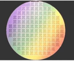
We provide custom thin film (silicon carbide) SiC epitaxy on 6H or 4H substrates for the development of silicon carbide devices. SiC epi wafer is mainly used for Schottky diodes, metal-oxide semiconductor field-effect transistors, junction field effect transistors, bipolar junction transistors, thyristors, GTO, and insulated gate bipolar.
PAM-XIAMEN is able to offer the following SiC reclaim wafer services.
Due to SiC physical and electronic properties,Silicon Carbide based device are well suitable for short wavelength optoelectronic, high temperature, radiation resistant, and high-power/high-frequency electronic devices,compared with Si and GaAs based device.
Xiamen Powerway offers InAs wafer - Indium arsenide which are grown by LEC(Liquid Encapsulated Czochralski) as epi-ready or mechanical grade with n type, p type or semi-insulating in different orientation(111)or(100).
PAM-XIAMEN is able to offer the following SiC reclaim wafer services.
FZ-Silicon The mono-crystalline silicon with the characteristics of low foreign-material content, low defect density and perfect crystal structure is produced with the float-zone process; no foreign material is introduced during the crystal growth. The FZ-Silicon conductivity is usually above 1000 Ω-cm, and the FZ-Silicon is mainly used to produce 1
PWAM Develops and manufactures compound semiconductor substrates-gallium arsenide crystal and wafer.We has used advanced crystal growth technology,vertical gradient freeze(VGF) and GaAs wafer processing technology,established a production line from crystal growth, cutting, grinding to polishing processing and built a 100-class clean room for 1
The etching wafer has the characteristics of low roughness, good glossiness and relatively low cost, and directly substitutes the polished wafer or epitaxial wafer which has relatively high cost to produce the electronic elements in some fields, to reduce the costs. There are the low-roughness, low-reflectivity and high-reflectivity etching wafers.
 Contact Information
 luna@powerwaywafer.compowerwaymaterial@gmail.com
  +86-592-5601 404