PWAM Develops and manufactures compound semiconductor substrates-gallium arsenide crystal and wafer.We has used advanced crystal growth technology,vertical gradient freeze(VGF) and GaAs wafer processing technology,established a production line from crystal growth, cutting, grinding to polishing processing and built a 100-class clean room for wafer cleaning and packaging. Our GaAs wafer include 2~6 inch ingot/wafers for LED,LD and Microelectronics applications.We are always dedicated to improve the quality of currently substates and develop large size substrates.
MOQ :
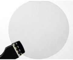
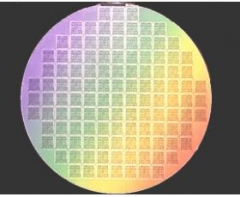
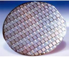
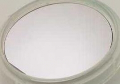
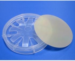
1(GaAs) Gallium Arsenide Wafers
PWAM Develops and manufactures compound semiconductor substrates-gallium arsenide crystal and wafer.We has used advanced crystal growth technology,vertical gradient freeze(VGF) and GaAs wafer processing technology,established a production line from crystal growth, cutting, grinding to polishing processing and built a 100-class clean room for wafer cleaning and packaging. Our GaAs wafer include 2~6 inch ingot/wafers for LED,LD and Microelectronics applications.We are always dedicated to improve the quality of currently substates and develop large size substrates.
(GaAs)Gallium Arsenide Wafers for LED Applications
|
Item |
Specifications |
Remarks |
|
Conduction Type |
SC/n-type |
SC/p-type with Zn dope Available |
|
Growth Method |
VGF |
|
|
Dopant |
Silicon |
Zn available |
|
Wafer Diamter |
2, 3 & 4 inch |
Ingot or as-cut availalbe |
|
Crystal Orientation |
(100)20/60/150 off (110) |
Other misorientation available |
|
OF |
EJ or US |
|
|
Carrier Concentration |
(0.4~2.5)E18/cm3 |
|
|
Resistivity at RT |
(1.5~9)E-3 Ohm.cm |
|
|
Mobility |
1500~3000cm2/V.sec |
|
|
Etch Pit Density |
<5000/cm2 |
|
|
Laser Marking |
upon request |
|
|
Surface Finish |
P/E or P/P |
|
|
Thickness |
220~450um |
|
|
Epitaxy Ready |
Yes |
|
|
Package |
Single wafer container or cassette |
|
(GaAs)Gallium Arsenide Wafers for LD Applications
|
Item |
Specifications |
Remarks |
|
Conduction Type |
SC/n-type |
|
|
Growth Method |
VGF |
|
|
Dopant |
Silicon |
|
|
Wafer Diamter |
2, 3 & 4 inch |
Ingot or as-cut available |
|
Crystal Orientation |
(100)20/60/150 off (110) |
Other misorientation available |
|
OF |
EJ or US |
|
|
Carrier Concentration |
(0.4~2.5)E18/cm3 |
|
|
Resistivity at RT |
(1.5~9)E-3 Ohm.cm |
|
|
Mobility |
1500~3000 cm2/V.sec |
|
|
Etch Pit Density |
<500/cm2 |
|
|
Laser Marking |
upon request |
|
|
Surface Finish |
P/E or P/P |
|
|
Thickness |
220~350um |
|
|
Epitaxy Ready |
Yes |
|
|
Package |
Single wafer container or cassette |
|
(GaAs)Gallium Arsenide Wafers,Semi-insulating for Microelectronics Applications
|
Item |
Specifications |
Remarks |
|
Conduction Type |
Insulating |
|
|
Growth Method |
VGF |
|
|
Dopant |
Undoped |
|
|
Wafer Diamter |
2, 3 & 4 inch |
Ingot available |
|
Crystal Orientation |
(100)+/- 0.50 |
|
|
OF |
EJ, US or notch |
|
|
Carrier Concentration |
n/a |
|
|
Resistivity at RT |
>1E7 Ohm.cm |
|
|
Mobility |
>5000 cm2/V.sec |
|
|
Etch Pit Density |
<8000 /cm2 |
|
|
Laser Marking |
upon request |
|
|
Surface Finish |
P/P |
|
|
Thickness |
350~675um |
|
|
Epitaxy Ready |
Yes |
|
|
Package |
Single wafer container or cassette |
|
6" (GaAs)Gallium Arsenide Wafers,Semi-insulating for Microelectronics Applications
|
Item |
Specifications |
Remarks |
|
Conduction Type |
Semi-insulating |
|
|
Grow Method |
VGF |
|
|
Dopant |
Undoped |
|
|
Type |
N |
|
|
Diamater(mm) |
150±0.25 |
|
|
Orientation |
(100)00±3.00 |
|
|
NOTCH Orientation |
〔010〕±20 |
|
|
NOTCH Deepth(mm) |
(1-1.25)mm 890-950 |
|
|
Carrier Concentration |
N/A |
|
|
Resistivity(ohm.cm) |
>1.0×10⁷ or 0.8-9 x10⁻³ |
|
|
Mobility(cm2/v.s) |
N/A |
|
|
Dislocation |
N/A |
|
|
Thickness(µm) |
675±25 |
|
|
Edge Exclusion for Bow and Warp(mm) |
N/A |
|
|
Bow(µm) |
N/A |
|
|
Warp(µm) |
≤20.0 |
|
|
TTV(µm) |
≤10.0 |
|
|
TIR(µm) |
≤10.0 |
|
|
LFPD(µm) |
N/A |
|
|
Polishing |
P/P Epi-Ready |
|
2" LT-GaAs (Low Temperature-Grown Galium Arsenide) Wafer Specifications
|
Item |
Specifications |
Remarks |
|
Diamater(mm) |
Ф 50.8mm ± 1mm |
|
|
Thickness |
1-2um or 2-3um |
|
|
Marco Defect Density |
≤ 5 cm-2 |
|
|
Resistivity(300K) |
>108 Ohm-cm |
|
|
Carrier |
<0.5ps |
|
|
Dislocation Density |
<1x106cm-2 |
|
|
Useable Surface Area |
≥80% |
|
|
Polishing |
Single side polished |
|
|
Substrate |
GaAs Substrate |
|
* We also can provide poly crystal GaAs bar, 99.9999%(6N).
Remark:
The Chinese government has announced new limits on the exportation of Gallium materials (such as GaAs, GaN, Ga2O3, GaP, InGaAs, and GaSb) and Germanium materials used to make semiconductor chips. Starting from August 1, 2023, exporting these materials is only allowed if we obtains a license from the Chinese Ministry of Commerce. Hope for your understanding and cooperation!
We are manufacturing various types of epi wafer III-V silicon doped n-type semiconductor materials based on Ga, Al, In, As and P grown by MBE or MOCVD. We supply custom structures to meet customer specifications.please contact us for more information.
Xiamen Powerway offers GaP wafer - gallium Phosphide which are grown by LEC(Liquid Encapsulated Czochralski) as epi-ready or mechanical grade with n type, p type or semi-insulating in different orientation(111)or(100).
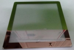
PAM-XIAMEN Offers photoresist plate with photoresist We can offer Nanolithography (photolithography):Surface preparation, Photoresist apply, Soft bake, Alignment, Exposure, Development,Hard bake, Develop inspect, Etch, Photoresist removal(strip), Final inspection.
Xiamen Powerway offers InSb wafer - Indium antimonide which are grown by LEC(Liquid Encapsulated Czochralski) as epi-ready or mechanical grade with n type, p type or semi-insulating in different orientation(111)or(100).
PAM-XIAMEN Offers Photomasks A photo mask is a thin coating of masking material supported by a thicker substrate, and the masking material absorbs light to varying degrees and can be patterned with a custom design. The pattern is used to modulate light and transfer the pattern through the process of photolithography which is the fundamental process1
PAM-XIAMEN has established the manufacturing technology for freestanding (gallium nitride)GaN substrate wafer, which is for UHB-LED and LD. Grown by hydride vapour phase epitaxy (HVPE) technology,Our GaN substrate has low defect density.
The etching wafer has the characteristics of low roughness, good glossiness and relatively low cost, and directly substitutes the polished wafer or epitaxial wafer which has relatively high cost to produce the electronic elements in some fields, to reduce the costs. There are the low-roughness, low-reflectivity and high-reflectivity etching wafers.
We are manufacturing various types of epi wafer III-V silicon doped n-type semiconductor materials based on Ga, Al, In, As and P grown by MBE or MOCVD. We supply custom structures to meet customer specifications.please contact us for more information.
 Contact Information
 luna@powerwaywafer.compowerwaymaterial@gmail.com
  +86-592-5601 404