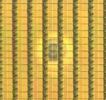
Indium Phosphide (InP) is a key semiconductor material that enables optical systems to deliver the performance required for data center, mobile backhaul, metro and long-haul applications. Lasers, photodiodes and waveguides fabricated on InP operate at the optimum transmission window of glass fiber, which enable efficient fiber communications. PAM-XIAMEN’s proprietary Etched Facet Technology (EFT) allows wafer level testing similar to traditional semiconductor manufacturing. EFT enables high yield, high performance and reliable lasers.

1)2"InP wafer
Orientation:±0.5°
Type/Dopant:N/S;N/Un-doped
Thickness:350±25mm
Mobility:>1700
Carrier Concentration:(2~10)E17
EPD:<50000cm^-2
Polished:SSP
2)1",2"InP wafer
Orientation:±0.5°
Type/Dopant:N/Un-doped
Thickness:350±25mm
Mobility:>1700
Carrier Concentration:(2~10)E17
EPD:<50000cm^-2
Polished:SSP
3)1",2"InP wafer
Orientation:A±0.5°
Type/Dopant:N/S;N/Un-doped
Thickness:350±25mm
Polished:SSP
4)2"InP wafer
Orientation:B±0.5°
Type/Dopant:N/Te;N/Undoped
Thickness:400±25mm;500±25mm
Polished:SSP
5)2"InP wafer
Orientation:(110)±0.5°
Type/Dopant:P/Zn;N/S
Thickness:400±25mm
Polished:SSP/DSP
6)2"InP wafer
Orientation:(211)B;(311)B
Type/Dopant:N/Te
Thickness:400±25mm
Polished:SSP/DSP
7)2"InP wafer
Orientation:(100)2°off+/-0.1 degree t.n. (110)
Type/Dopant:SI/Fe
Thickness:500±20mm
Polished:SSP
8)2" size InGaAs/InP epitaxial wafer,and we accept custom specs.
Substrate: (100) InP substrate
Epi Layer 1: In0.53Ga0.47As layer , undoped , thickness 200 nm
Epi Layer 2: In0.52Al0.48As layer , undoped , thickness 500 nm
Epi Layer 3:In0.53Ga0.47As layer , undoped , thickness 1000 nm
Top Layer :In0.52Al0.48As layer , undoped , thickness 50 nm
Xiamen Powerway Advanced Material Co., Ltd (PAM-XIAMEN) offers the highest purity InGaAs/InP Epitaxial Wafers in the industry today. Sophisticated manufacturing processes have been put in place to customize and produce high quality Indium Phosphide Epitaxial wafers up to 4 inches with wavelengths from 1.7 to 2.6μm, ideally suited for high speed, long wavelength imaging, high speed HBT and HEMTs, APDs and analog-digital converter circuits. Applications using InP-based components can greatly exceed transmission rates in comparison to similar components structured on GaAs or SiGe based platforms.
Relative products:
InAs wafer
InSb wafer
InP wafer
GaAs wafer
GaSb wafer
GaP wafer
Source: semiconductorwafers.net
For more information, please visit our website:http://www.semiconductorwafers.net,
send us email at angel.ye@powerwaywafer.com or powerwaymaterial@gmail.com.
 Contact Information
 luna@powerwaywafer.com
 powerwaymaterial@gmail.com
  +86-592-5601 404